By Peter Zaballos
TALES FROM THE EARLY-ISH DAYS OF SILICON VALLEY
The early 1980s were a sort of a “between” era in semiconductors – between the era of predominantly manual chip design and fabrication and the era of computer-driven design and highly automated production.
One awesome aspect of working at LSI Logic in this “between” era was that so many of the founders and executives there had been in the semiconductor industry from the very beginning of its existence, or pretty darn close to the beginning. And they had stories to tell as they helped propel the industry forward.
In my first year at LSI I was in a meeting with Wilf Corrigan (co-founder/CEO) and a small group of executives from one of our customers – they were there to check out our fab and processes. One of these visiting executives was someone Wilf had worked with ages ago.
At a break in the meeting he and Wilf started swapping stories of the early days of the industry, back when he was a manufacturing engineer. He said something like “do you remember when we were at Transitron, and we’d hold the wafers with tweezers, dip them in acid to etch them, and then look at the second hand on the wall clock to time how long to keep them in the acid bath?”
Then they both laughed long and hard. Because that’s how they made semiconductors in the 1960s.
In the 1960s and 1970s semiconductor manufacturing was still largely manual. Wafers were literally carried from one manufacturing step to the next. Photolithography machines were manually set up, aimed, and operated.
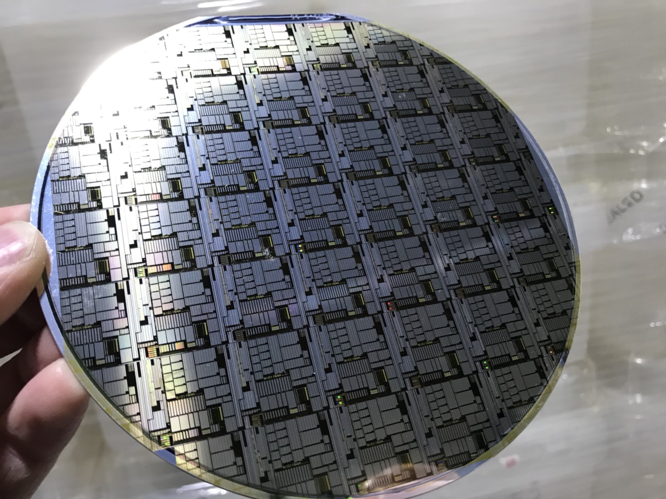
In the 1980s all of that started to change. As a result of Moore’s law, the line widths of semiconductor traces were steadily shrinking, the density of devices per wafer were increasing, and the size of the wafers were themselves increasing – from 4 inch diameters in 1975, to 6 inch diameters in the early 1980s – to today’s 18 inch diameter wafers. And the reasoning is pure economics – an 18 inch wafer can produce 200x more chips than a 4 inch wafers.
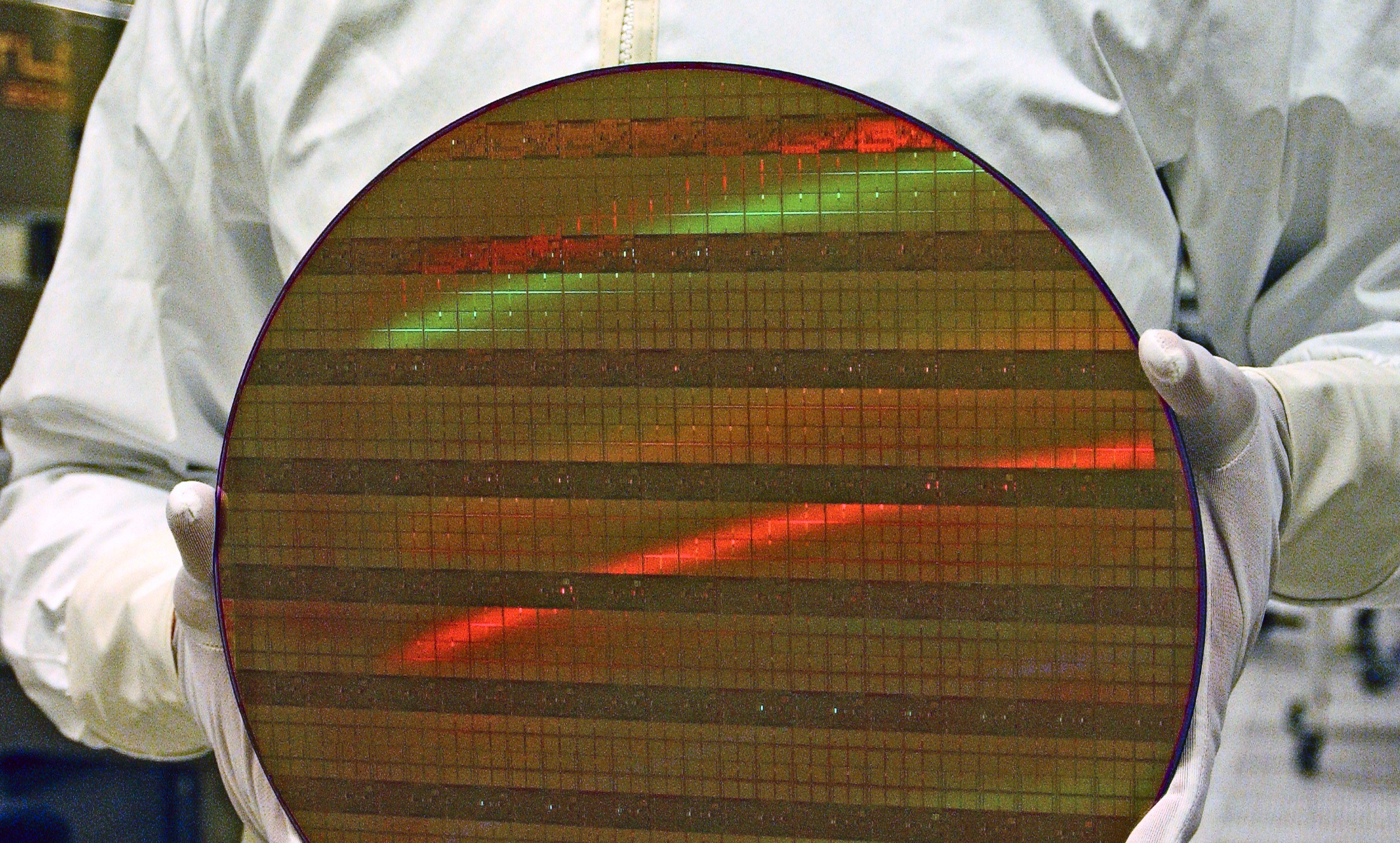
This also meant that fabs had to get much cleaner. Contaminants smaller than specs of dust could get in the way of a photolithography trace or cause a short between two metal lines and as wafer sizes grew, process variations or human error were that much more prevalent.
So conditions you could tolerate in a fab in 1975 would cause serious manufacturing yield problems in the factories of the 1980s. This is when the concept of a “clean room” took hold – a manufacturing environment with a system that could control the amount and size of airborne particles.
That latter metric – size of particle – would become super important. In the early 1980s Class 10 fabs were just becoming necessary – so in a cubic foot of air in the fab, there could only be 10 particles whose size is 0.5 microns. Class 1 fabs were being talked about, but no one could afford them in the 1980s.
Today, clean rooms are orders of magnitude cleaner than Class 1.
This is also when “bunny suits” became mandatory. It was when automated wafer transport systems were just coming on line, so wafers could be stacked in sealed “boats” and these could be transported between manufacturing stations and removed only when the wafer was being operated on.
Back in the mid-1980s wafer defects were pretty evenly caused by airborne contamination (airborne particles), process errors, equipment errors, and human error. This has changed a lot, today automation has almost completely eliminated human error, and technology has almost completely eliminated airborne contamination.

Final yield ultimately determined how many chips met the specification the customer had ordered. Poor yield meant they were getting less than they expected – and would have to make some painful adjustments to their own manufacturing schedules and revenue plans. Good yield meant we could either sell the customer the excess or stockpile them for follow-on orders.
Back to the stories.
In my second year at LSI we hired a super talented VP of Manufacturing, Travis White. He was a talkative and friendly Texan and loved to wander into the cubicle area where the marketing folks were and tell us stories about “way back when.”
I remember him telling us a story about when he was running a fab for Texas Instruments, and their yield suddenly plummeted. It was a true crisis and he and his team spent days and weeks analyzing their manufacturing data and processes and couldn’t figure it out. They were running out of ideas and understandably, the CEO and TI’s customers were getting impatient. They’d gone through all their processes, checked all the machinery, again and again. But could not find what was killing their yield.
So Travis walked down to the fab and just spent time looking around, observing.
And then he saw it.
They’d changed suppliers of semiconductor boats and needed to secure them with rubber bands. And a well intentioned supervisor had gone out and purchased a container of rubber bands for each work station.
Rubber bands dusted with talc. To make the bands easier to pick up.
And with every ‘snap” those talc particles were floating through the air, finding their way onto the wafers. That was what was killing yield.
Travis was as horrified as he was amused that something that simple could wreak such havoc, and go unnoticed.
He could wander into the marketing area because we literally had a semiconductor fab attached to our building in Milpitas, CA. In fact, the fab was the majority of the building.
It was a key selling point for our customers. We could walk them to the back of the office portion of the building and they could look through observation windows to see a few steps of the manufacturing going on, with all the employees busy at work. Some of our competitors couldn’t afford their own fabs, or had other companies make their custom semiconductors. But we had our own fab and controlled that part of our destiny.
More generally back then there were lots of semiconductor fabs in the valley – AMD, Intel, HP, MMI, National Semiconductor and dozens of others. That’s where the “silicon” of silicon valley came from.
I believe only Intel has a fab in Silicon Valley today. Everyone else stared down the face of the multi-billion dollar investments required to stay on the leading edge of semiconductor technology and outsourced their manufacturing to a small number of companies in Asia who act as “foundries” – you give them your design and they make the finished chips. Companies like TSMC and Samsung.
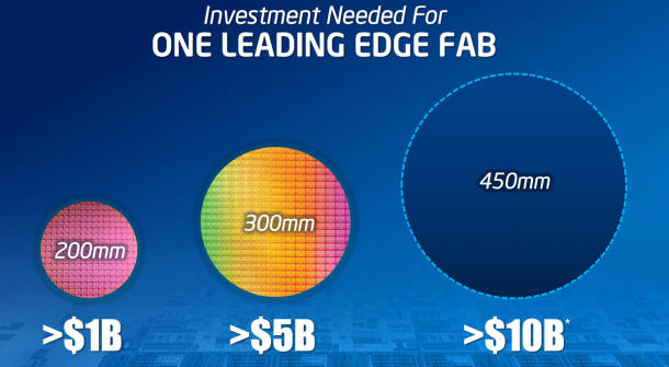
Even Intel is staggered at the expense required to build state-of-the-art semiconductor processes and fabs, and has recently acknowledged it can’t compete with these foundries. They themselves may start using them, or be faced with some serious investments to keep up.
So I frequently think back to Travis White’s stories and Wilf’s stories. It was awesome to be working with them when this industry was truly growing up. A small window of time at a point of significant industry transformation.
To this day I smile when I come across a rubber band that has talcum powder on it. Or see a wall clock and think of Wilf Corrigan, holding a wafer with tweezers checking the second hand on that clock.
Tags: Moore's law, rubber bands, semiconductor fabs, wall clocks

January 7, 2025 at 7:38 am |
[…] after taking a job at LSI Logic (see earlier posts on that company here, here, here, here, and here) and simply needed reliable […]
LikeLike